Why Are Microled Monitors So Expensive
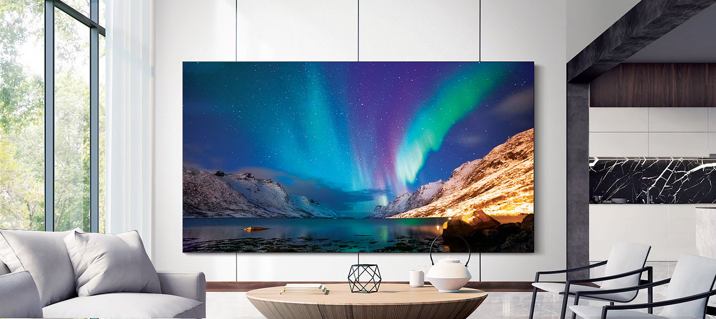
If you've been eyeing the next big thing in displays, you've probably asked yourself why are microled monitors so expensive after seeing those wild six-figure price tags. The short answer is that building a display out of millions of individually addressable microscopic LED chips is a manufacturing nightmare compared to how LCD or OLED panels roll off production lines.
The deeper answer involves yield rates below 50 percent, red LED efficiency losses at microscopic sizes, and a global infrastructure that LCD and OLED have spent decades perfecting while MicroLED is still figuring out the basics. As of 2026, a single square meter of finished MicroLED display can cost between $10,000 and $15,000, and that's before you even get to consumer monitor pricing. Let's break down exactly where that money goes.
Quick Answer: Why MicroLED Monitors Cost So Much
MicroLED monitors cost so much because manufacturing them requires transferring millions of microscopic LED chips onto a single substrate with near-perfect accuracy. Current production yield rates hover between 20 and 50 percent, meaning half or more of every batch gets discarded. Red LED chips also lose significant efficiency at MicroLED dimensions, driving up material and binning costs.
Finally, the supply chain for LCD and OLED displays has decades of infrastructure behind it, while MicroLED still lacks the scale to bring prices down.
The Core Problem: Building Millions of Perfect Tiny Lights
Why this isn't just "new tech is expensive"
Every new display technology starts expensive. LCD TVs were absurdly priced in the early 2000s. OLED monitors carried a massive premium for years.
But MicroLED faces a fundamentally different kind of problem. It's not just that the factories are new or the tooling is expensive. It's that the basic physics of making millions of tiny, individual light-emitting chips and getting them all to work on one panel is brutally difficult at scale.
Think of it this way. A 4K MicroLED monitor has roughly 25 million individual LED chips (one red, one green, and one blue sub-pixel for each of the 8.3 million pixels). Every single one of those 25 million chips needs to be manufactured, tested, transferred to the substrate, bonded electrically, and then verified as functional.
If even 0.1 percent of them fail, you've got 25,000 dead sub-pixels on your panel. That's not a display you can sell.
The yield rate reality most articles skip
Yield rate is the percentage of finished panels that meet quality standards, and it's the single biggest cost driver in MicroLED production. In our research, aggregate industry reports suggest current MicroLED yield rates sit somewhere between 20 and 50 percent for large-format displays. That means for every two panels that start the production line, only one comes out functional enough to sell.
This isn't a minor inefficiency. It's a fundamental cost multiplier. If your yield rate is 50 percent, you're effectively paying double for every component and every minute of manufacturing time.
At 25 percent yield, you're quadrupling your costs. And those costs get passed directly to the buyer.
The yield problem gets worse as pixel density increases. A large-format signage display with relatively large pixels (1mm or more between them) has better yield rates than a monitor with tight pixel pitch. That's why MicroLED has found its first commercial foothold in big, low-pixel-density applications like video walls, not in desktop monitors where the chips need to be smaller and the tolerances tighter.
How OLED competition makes MicroLED's cost problem harder to solve
Here's the part that doesn't get enough attention. MicroLED isn't just fighting its own manufacturing challenges. It's competing against OLED, which has been on a steady cost-decline curve for over a decade.
LG Display's WOLED panels have gotten cheaper every year. Samsung's QD-OLED has added another competitive pressure. Mini-LED backlit LCDs have emerged as a "good enough" middle ground for most consumers.
Every dollar that goes into improving OLED or Mini-LED manufacturing is a dollar that MicroLED can't benefit from. The display industry has poured hundreds of billions into OLED infrastructure. MicroLED is trying to build a parallel supply chain from scratch while its main competitor keeps getting more cost-efficient.
That dynamic makes it incredibly hard for MicroLED to reach the production volumes needed to drive prices down.
How MicroLED Actually Works (And Where Cost Hides)
What makes MicroLED different from every other display
MicroLED is an emissive display technology, meaning each pixel produces its own light. OLED works the same way. The difference is material.
OLED uses organic compounds that degrade over time. MicroLED uses inorganic gallium nitride (GaN) LEDs, the same basic technology you'd find in a household LED bulb, just shrunk down to less than 50 micrometers across.
This inorganic approach gives MicroLED some real advantages. No burn-in risk. Higher peak brightness potential.
Better power efficiency at high brightness levels. Longer theoretical lifespan. But the manufacturing process is completely different from anything the display industry has done at scale before.
LCD works by shining a backlight through liquid crystal shutters. OLED works by depositing organic material through fine metal masks or inkjet printing. Neither requires placing millions of individual semiconductor chips onto a substrate with micron-level precision.
MicroLED does, and that's where the cost lives.
The three-chip RGB problem at microscopic scale
Every MicroLED pixel requires three separate LED chips: one red, one green, and one blue. Each of these chips is made from slightly different semiconductor materials and has slightly different electrical and optical characteristics. Green and blue LEDs use GaN efficiently.
Red LEDs use a different material system (typically AlGaInP or GaAs-based structures) that behaves very differently when you shrink it down.
This means you're not just manufacturing one type of chip. You're manufacturing three different types, each with its own process parameters, its own defect rates, and its own efficiency curves. Then you have to place all three in the correct position for every single pixel, millions of times over, on one panel.
The complexity multiplies fast.
Why red LED chips are the secret bottleneck nobody talks about
Red MicroLED chips are the Achilles' heel of the entire technology. When you shrink a red LED down to MicroLED dimensions (below 50 micrometers), its external quantum efficiency drops dramatically. Industry data suggests efficiency losses of 40 percent or more at the 20 to 25 micrometer chip size range needed for high-density displays.
This happens because of something called sidewall recombination. At tiny sizes, a much larger proportion of the chip's surface area is near the edges, where defects trap electrons and holes before they can produce light. The smaller the chip gets, the worse this effect becomes.
Red LEDs suffer from it far more than green or blue.
The practical impact is that red MicroLED chips need to be driven harder to produce the same brightness, which generates more heat and reduces lifespan. Manufacturers either accept lower red brightness (throwing off color balance) or bin aggressively for the few chips that perform well (driving up costs). Either way, red LED efficiency is a major reason MicroLED panels cost what they do.
The Mass Transfer Bottleneck Explained
What mass transfer actually means
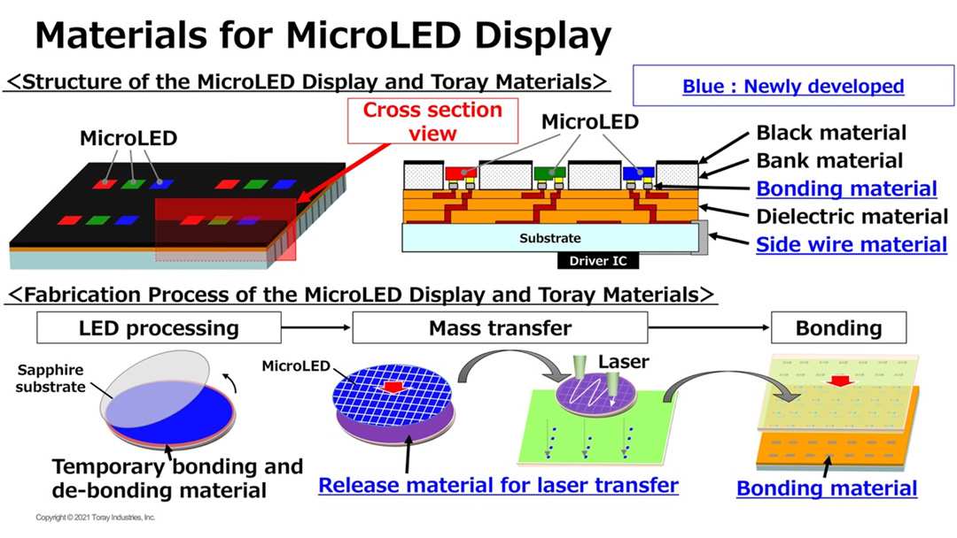
Mass transfer is the process of picking up millions of individual MicroLED chips from their growth wafer and placing them onto the display substrate in exactly the right positions. It sounds straightforward. In practice, it's one of the hardest manufacturing challenges in modern electronics.
Each chip is smaller than a human hair. You need to pick them up without damaging them, align them to bonding pads with micron-level accuracy, and bond them electrically and mechanically. Then you need to do this for every single chip on the panel, millions of times, in a reasonable amount of time.
Current mass transfer tools can handle roughly 10 million chips per hour for signage-grade applications. For high-density monitor panels, the speed drops and the precision requirements go up simultaneously.
Why moving millions of chips sounds simple but isn't
The physics of handling objects at this scale is counterintuitive. At micrometer dimensions, electrostatic forces, van der Waals forces, and surface tension dominate over gravity. Chips stick to surfaces they shouldn't.
They clump together. They shift position during transfer. A fraction of a micron of misalignment can render a pixel non-functional.
Then there's the sheer statistical challenge. Even if your transfer process is 99.9 percent accurate, you're still placing 25 million chips on a 4K panel. That's 25,000 potential failures per panel.
At 99.99 percent accuracy, you're down to 2,500. Getting to the 99.999 percent accuracy needed for a sellable consumer display requires process control that the industry hasn't achieved yet at production scale.
Transfer speed vs. yield: the tradeoff killing profitability
Faster transfer speeds mean more panels per hour, which means lower per-panel equipment costs. But faster speeds also mean more placement errors, which means lower yield rates. Slower speeds improve yield but kill throughput.
This tradeoff is the central economic problem of MicroLED manufacturing.
Current production lines are still optimizing this balance. Samsung, Sony, and several Chinese manufacturers have invested heavily in mass transfer equipment, but the sweet spot between speed and yield for consumer-grade monitor panels hasn't been found yet. Until it is, every panel produced carries the cost of this unresolved optimization problem.
Stamp-based, laser, and fluidic methods compared
There are three main approaches to mass transfer, each with different tradeoffs.
| Method | How It Works | Speed | Yield | Best For |
|---|---|---|---|---|
| Stamp-based (elastomer) | Picks up chips using patterned sticky surface | Moderate | Moderate | Medium-density panels |
| Laser-assisted | Laser lifts chips from wafer, substrate catches them | Fast | Variable | Large-format signage |
| Fluidic self-assembly | Chips suspended in fluid, aligned by surface tension patterns | Potentially fast | Still developing | High-volume future production |
Stamp-based methods are the most mature but struggle with throughput at monitor-scale pixel densities. Laser-assisted transfer is fast but can damage chips during the lift-off process. Fluidic self-assembly is promising for future high-volume production but is still largely in the R&D phase as of 2026.
No single method has emerged as the clear winner, which means manufacturers are investing in multiple approaches simultaneously, further fragmenting the supply chain.
Real Numbers: What Actually Drives the Price
Yield rates in current production
Let's put concrete numbers on the yield problem. Industry analyses and manufacturer disclosures suggest the following approximate yield rates for MicroLED production as of 2026:
- Large-format signage (pixel pitch > 1.5mm): 40 to 60 percent yield
- Medium-format displays (pixel pitch 0.7 to 1.5mm): 25 to 40 percent yield
- High-density monitors (pixel pitch < 0.7mm): 15 to 30 percent yield
These numbers come from aggregate industry reporting and analyst estimates, not from any single manufacturer's public disclosure. The trend is clear: as pixel density increases, yield drops. And monitors require the highest pixel density of any MicroLED application.
Cost per LED chip before and after transfer losses
A raw MicroLED chip costs somewhere between $0.02 and $0.10 to manufacture at the wafer level, depending on size and color. That sounds cheap until you factor in transfer losses, bonding failures, and binning for color and brightness uniformity. After all processing, the effective cost per functional chip on a finished panel can be $2 to $20 or more, depending on the panel and the yield rate.
For a 4K monitor with 25 million sub-pixels, even at the low end of effective chip cost, you're looking at $50 million in raw chip costs per panel at 100 percent yield. At 25 percent yield, that's $200 million. Obviously, the actual economics work differently because defective chips are identified and managed during production rather than after final assembly.
But the cost multiplication from yield loss is real and massive.
Defect detection and repair economics
After mass transfer, every panel needs to be inspected for dead or defective pixels. This requires automated optical inspection systems that can scan millions of bonds and identify failures. Then comes the repair phase, which involves removing defective chips and replacing them.
Repair is expensive and time-consuming. Each repair requires precise laser removal of the failed chip, cleaning of the bonding pad, and placement of a replacement. For a panel with thousands of defects, repair can take hours.
At some point, the cost of repair exceeds the value of the panel, and it gets scrapped. This scrap rate is another major cost driver that gets baked into the price of every panel that does make it through.
What Samsung The Wall and Sony Crystal LED actually cost
Samsung's The Wall is the most commercially available MicroLED product. Its modular panels cost roughly $10,000 to $15,000 per square meter as of 2026, depending on pixel pitch and configuration. A full 110-inch 4K installation runs well into six figures.
Sony's Crystal LED (CLEDIS) targets the enterprise and professional market with similar pricing. A 16K Crystal LED system for a virtual production studio can cost $500,000 or more. These aren't consumer products.
They're commercial installations sold to businesses that need the specific advantages MicroLED offers and are willing to pay for them.
Neither Samsung nor Sony has released a consumer MicroLED monitor. The Odyssey line uses Mini-LED backlighting, not true MicroLED. This tells you everything about where the technology stands for desktop use.
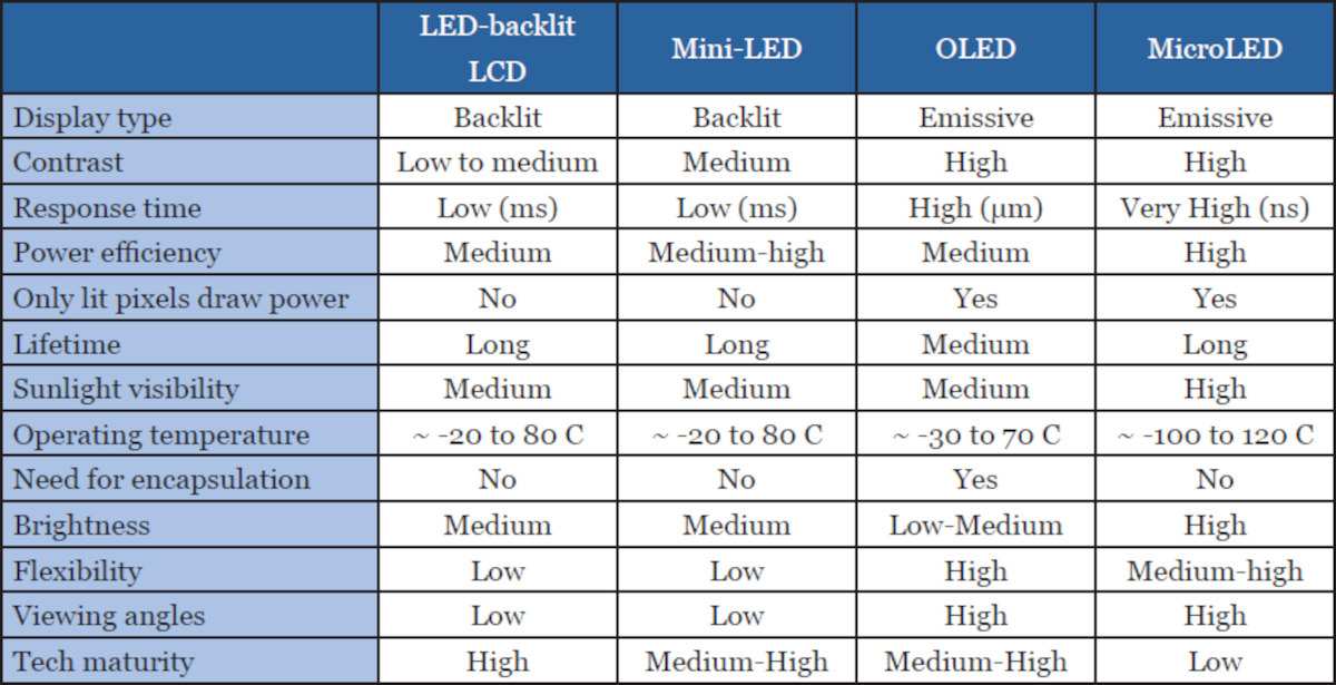
Image source: Bing (Web (fair-use with source credit))

Image source: Bing (Web (fair-use with source credit))

Similar Posts