Why Are Microled Monitors Delayed
If you've been waiting for a MicroLED monitor on your desk, you're probably wondering what's taking so long. Understanding why are microled monitors delayed comes down to one core problem: the manufacturing process isn't ready for the pixel density a monitor demands. We've been tracking this space for years, and the gap between trade show demos and something you can actually buy is still enormous.
A 27" 4K MicroLED panel requires over 24 million individual LED chips to be placed perfectly on a substrate. Even at 99.99% yield, that leaves thousands of dead pixels per panel. As of 2026, the industry hasn't solved this at a cost or scale that makes consumer monitors realistic.
Let's break down exactly what's happening.
Quick Answer
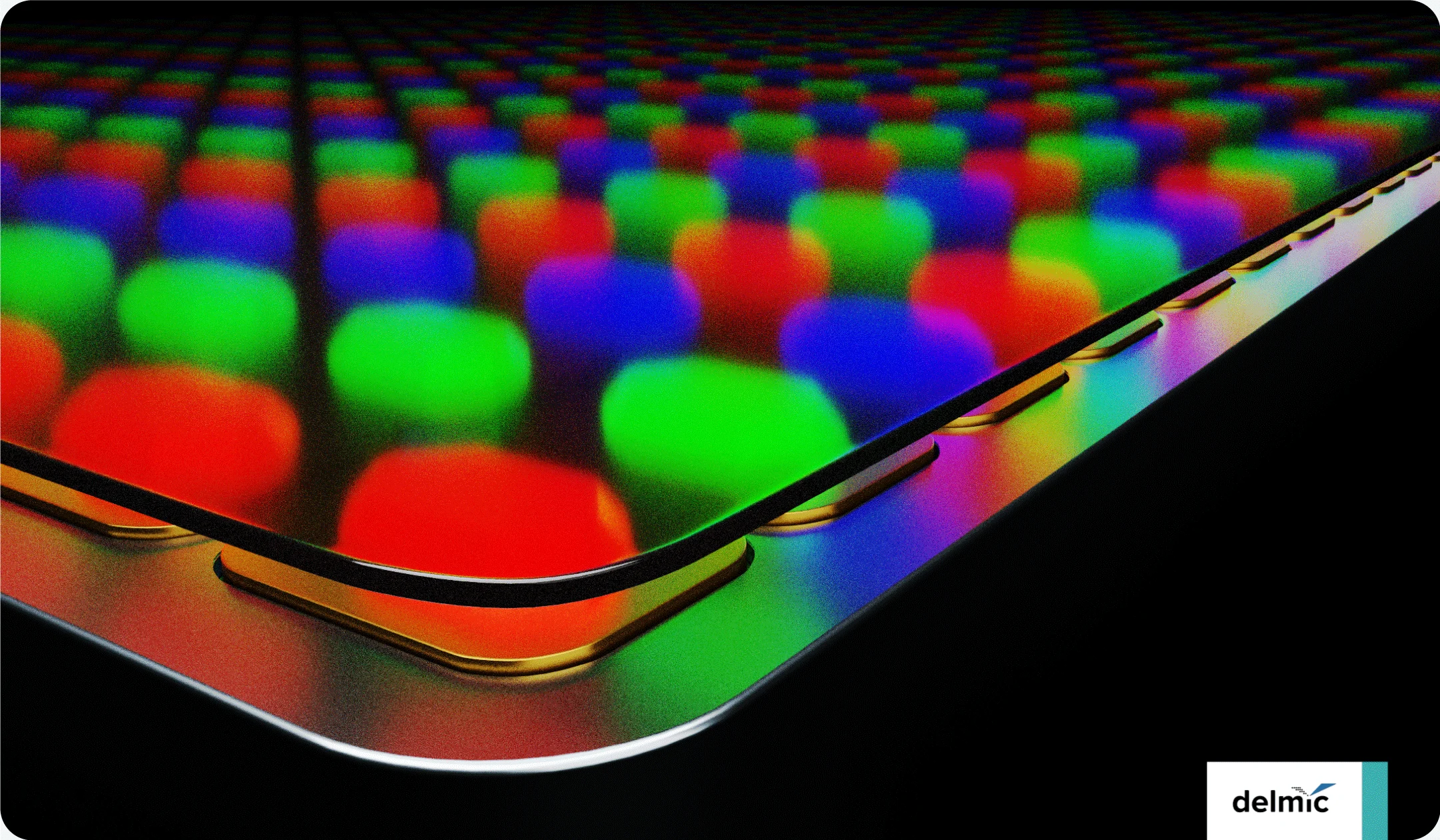
MicroLED monitors face delays because mass manufacturing can't achieve the required yield rates for high pixel density panels. Mass transfer of millions of microscopic LED chips creates too many defects per panel. Production costs run ten to thirty times higher than equivalent OLED displays.
Consumer-grade monitors likely won't arrive before 2028 to 2029 at the earliest. Current MicroLED products target large-format commercial installations where higher costs are acceptable.
What MicroLED Actually Promises
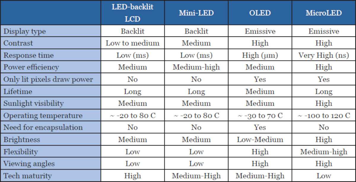
MicroLED is an emissive display technology. Each pixel is its own tiny inorganic LED that produces its own light. No backlight needed.
No liquid crystals. No organic compounds that degrade over time.
On paper, it's everything you'd want in a display.
- Perfect blacks, each pixel turns completely off, same as OLED
- Extreme brightness, 2,000 to 5,000+ nits, far beyond OLED's practical limits
- Zero burn-in, inorganic LEDs don't suffer the organic degradation that plagues OLED
- Wide color gamut, potential for near-full Rec. 2020 coverage
- Low power consumption, no backlight wasting energy
- Long lifespan, LED degradation measured in decades, not years
- Modular design, panels can be tiled together for custom sizes
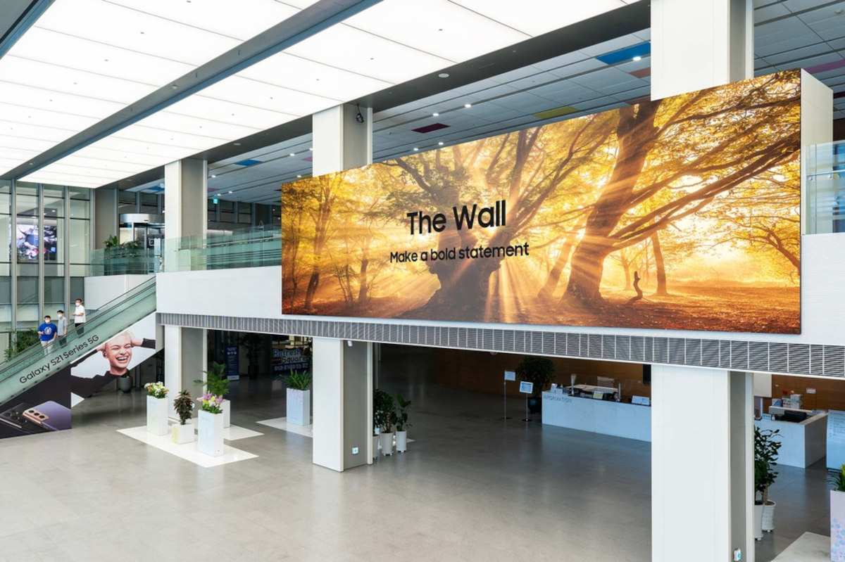
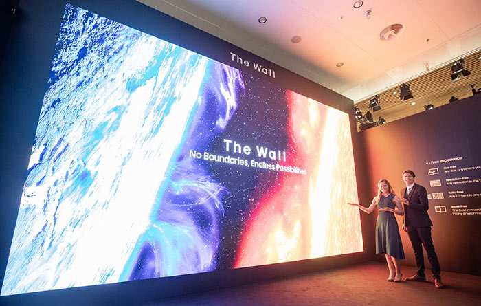
This sounds like the obvious next step past OLED. And for large TV-sized panels, it kind of is. Samsung's The Wall and Sony's Crystal LED exist.
You can buy them if you have the budget.
But shrink that technology down to a 27" or 32" monitor with 4K resolution? That's where everything falls apart. The physics don't scale the way manufacturers hoped.
The Mass Transfer Bottleneck
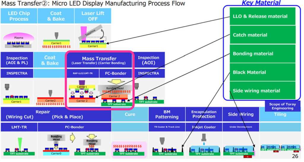
Here's the fundamental manufacturing challenge. Making a MicroLED panel means taking millions of microscopic LED chips from a growth wafer and placing them precisely onto a glass or silicon substrate. This is called mass transfer.
For a 4K monitor at 27", you're dealing with roughly 24 million individual LED dies. That's 3840 × 2160 pixels, and each pixel needs three sub-pixels (red, green, blue). Each die is smaller than a human hair.
Some are under 30 micrometers.
Now place all 24 million of them. Perfectly. In one pass.
Current mass transfer approaches include several methods. Laser-assisted transfer uses a laser to release chips from the carrier wafer onto the substrate. Elastomer stamp transfer works like a rubber stamp picking up and placing chips.
Fluidic self-assembly suspends chips in fluid and lets them settle into pockets on the substrate. Electrostatic transfer uses electric fields to move chips.
Each method has trade-offs between speed, precision, and yield.
| Transfer Method | Speed | Precision | Maturity Status |
|---|---|---|---|
| Elastomer stamp | Moderate | Good | In production for large panels |
| Laser-assisted | Slow | Excellent | R&D / limited production |
| Fluidic self-assembly | Potentially fast | Moderate | Early R&D stage |
| Electrostatic transfer | Moderate | Good | Pilot phase |
None of these methods currently operates at the speed and precision needed for consumer monitor production. The equipment wasn't designed for this. The entire supply chain around MicroLED mass transfer is still being invented while companies try to productionize it.
Yield Rates: The Math That Monitors Can't Clear
Let's talk about yield. This is the real killer.
A manufacturer needs better than 99.999% yield per pixel for a monitor to be viable. That's five nines. At 99.999%, a 4K panel has roughly 8 dead pixels across the entire display.
That's repairable or within acceptable tolerance for most standards.
Current mass transfer processes in production are achieving around 99.9% to 99.99%. That's two to four nines. Looks close until you do the math.
At 99.99% yield, a 4K panel has about 800 dead pixels. That's dead pixels scattered randomly across the screen. Unsellable.
At 99.9% yield? Around 8,000 dead pixels. That's not a display, that's a nightmare.
The problem compounds because monitors have much higher pixel density than TVs. A 76" 4K TV has the same 24 million pixels as a 27" monitor. But the TV spreads those pixels over a much larger area.
Each individual chip can be slightly larger. The placement tolerance is slightly more forgiving. The substrate area is larger, so you have more room to work with.
A monitor crams those same 24 million pixels into a much smaller space. Smaller chips. Tighter tolerances.
More things can go wrong per square inch.
And then there's the repair problem. If a chip is defective after transfer, you need to remove it and replace it. For a TV with a few dead pixels, maybe that's manageable.
For a monitor with hundreds or thousands of defects, you'd essentially need to redo the entire panel.
This is why yield rate matters so much more for monitors than TVs. The tolerance window is razor thin.
Production cost scales inversely with yield. A panel that passes at 99.999% costs a certain amount to make. A panel that fails at 99.99% costs the same to make and is worthless.
Manufacturers eat that cost. The consumer pays for it.
 -Reviewer-Photo-SOURCE-Brad-Bourque.jpg)

Similar Posts